 | ÐлекÑÑоннÑй компоненÑ: EL7154CS | СкаÑаÑÑ:  PDF PDF  ZIP ZIP |
Äîêóìåíòàöèÿ è îïèñàíèÿ www.docs.chipfind.ru
EL7154C
January
1996
Rev
B
EL7154C
High Speed Monolithic Pin Driver
Note All information contained in this data sheet has been carefully checked and is believed to be accurate as of the date of publication however this data sheet cannot be a ``controlled document'' Current revisions if any to these
specifications are maintained at the factory and are available upon your request We recommend checking the revision level before finalization of your design documentation
1995 Elantec Inc
Features
Comparatively low cost
3-State output
3V and 5V Input compatible
Clocking speeds up to 10 MHz
20 ns Switching delay time
4A Peak drive
Isolated drains
Low output impedance
2 5
X
Low quiescent current
5 mA
Wide operating voltage
4 5V 16V
Isolated P-channel device
Separate ground and V
L
pins
Applications
Loaded circuit board testers
Digital testers
Level shifting below GND
IGBT drivers
CCD drivers
Ordering Information
Part No
Temp Range
Pkg
Outline
EL7154CN b40 C to a85 C 8-Pin P-DIP MDP0031
EL7154CS b40 C to a85 C 8-Pin SOIC
MDP0027
Nominal Operating
Voltage Range
Pin
Min
Max
V
L
b
3
0
V
DD
V
L
5
15
V
H
V
L
2
15
V
DD
V
H
b
0 5
15
V
DD
5
15
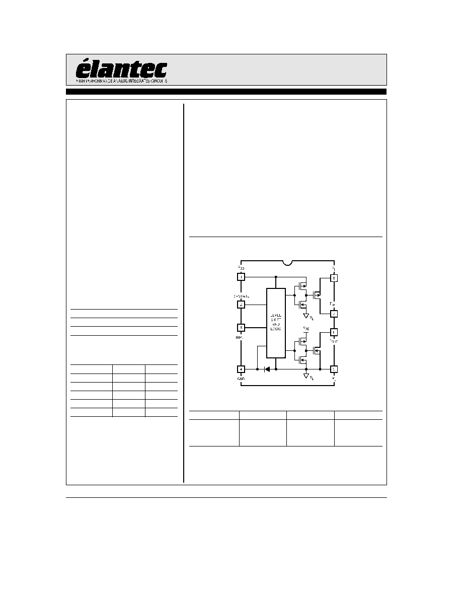
General Description
The EL7154C 3-state pin driver is particularly well suited for
ATE and level shifting applications The 4A peak drive capabil-
ity makes the EL7154C an excellent choice when driving high
speed capacitive lines
The p-channel MOSFET is completely isolated from the power
supply providing a high degree of flexibility Pin (7) can be
grounded and the output can be taken from pin (8) when a
``source follower'' output is desired Then n-channel MOSFET
has an isolated drain but shares a common bus with pre-drivers
and level shifter circuits This is necessary to ensure that the
n-channel device can turn off effectively when V
L
goes below
GND In some power-FET and IGBT applications negative
drive is desirable to insure effective turn-off The EL7154 can be
used in these applications by returning V
L
to a moderate nega-
tive potential
Connection Diagram
7154 1
Top View
Truth Table
3-State
Input
P
OUT
N
OUT
0
0
Open
Open
0
1
Open
Open
1
0
HIGH
Open
1
1
Open
LOW
Manufactured
under
U S
Patent
Nos
5 334 883
5 341 047
5 352 578
5 352 389
5 351 012
5 374 898
EL7154C
High Speed Monolithic Pin Driver
Absolute Maximum Ratings
Supply (V
DD
to V
L
V
H
V
L
V
H
to GND)
V
a
to V
H
16 5V
V
L
to GND
b
5V
Input Pins
b
0 3V below V
L
to
a
0 3V above V
DD
Peak Output Current
4A
Storage Temperature Range
b
65 C to
a
150 C
Ambient Operating Temperature
b
40 C to
a
85 C
Operating Junction Temperature
125 C
Power Dissipation
SOIC
570 mW
PDIP
1050 mW
Important Note
All parameters having Min Max specifications are guaranteed The Test Level column indicates the specific device testing actually
performed during production and Quality inspection Elantec performs most electrical tests using modern high-speed automatic test
equipment specifically the LTX77 Series system Unless otherwise noted all tests are pulsed tests therefore T
J
e
T
C
e
T
A
Test Level
Test Procedure
I
100% production tested and QA sample tested per QA test plan QCX0002
II
100% production tested at T
A
e
25 C and QA sample tested at T
A
e
25 C
T
MAX
and T
MIN
per QA test plan QCX0002
III
QA sample tested per QA test plan QCX0002
IV
Parameter is guaranteed (but not tested) by Design and Characterization Data
V
Parameter is typical value at T
A
e
25 C for information purposes only
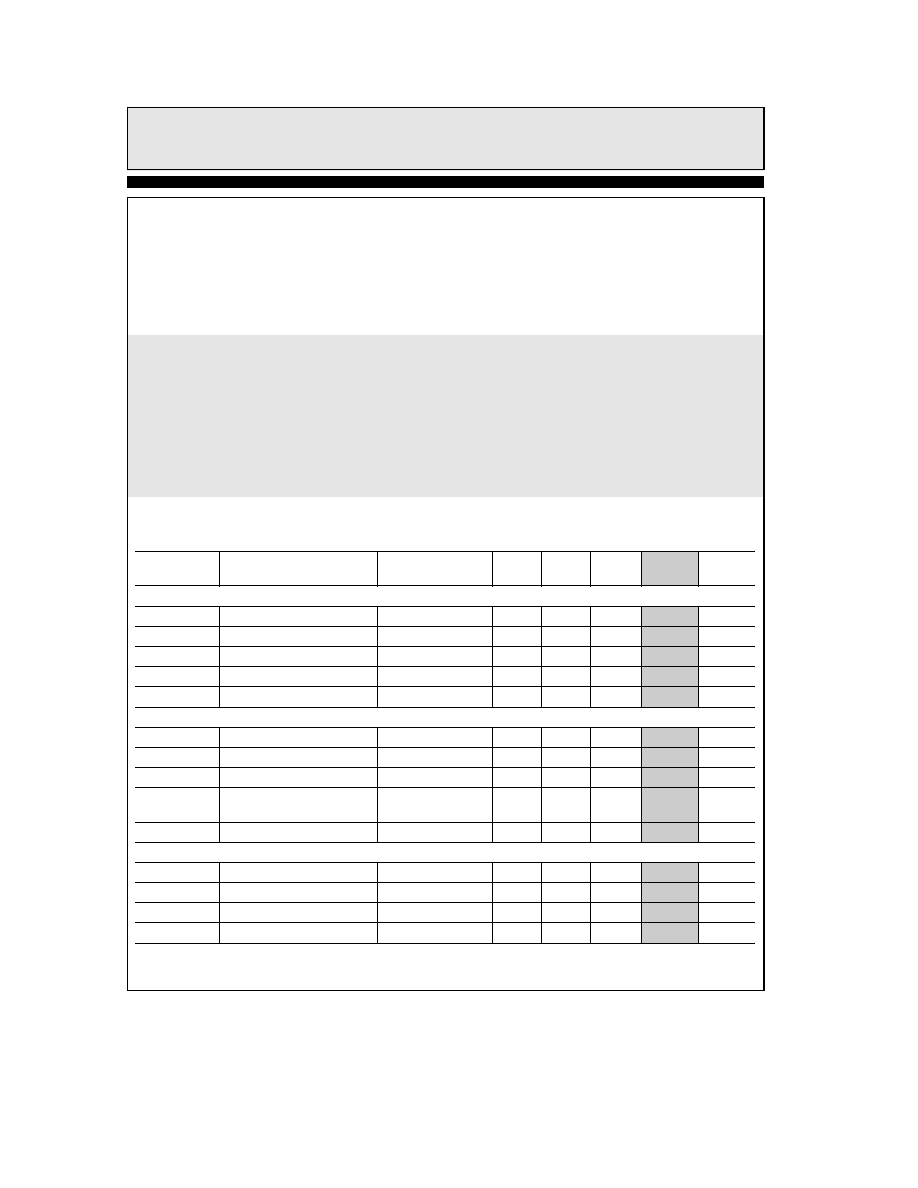
DC Electrical Characteristics
T
A
e
25 C V
DD
e a
12V V
H
e a
12V V
L
e b
3V unless otherwise specified
Parameter
Description
Test
Min
Typ
Max
Test
Units
Conditions
Level
Input
V
IH
Logic ``1'' Input Voltage
2 4
I
V
I
IH
Logic ``1'' Input Current
V
IH
e
V
DD
0 1
10
I
mA
V
IL
Logic ``0'' Input Voltage
0 6
I
V
I
IL
Logic ``0'' Input Current
V
IL
e
0V
0 1
10
I
mA
V
HVS
Input Hysteresis
0 3
V
V
Output
R
OH
Pull-Up Resistance
I
OUT
e b
100 mA
1 5
4
I
X
R
OL
Pull-Down Resistance
I
OUT
e a
100 mA
2
4
I
X
I
OUT
Output Leakage Current
V
DD
GND
0 2
10
I
mA
I
PK
Peak Output Current
Source
4 0
V
A
Sink
4 0
I
DC
Continuous Output Current
Source Sink
200
I
mA
Power Supply
I
S
Power Supply Current
Inputs
e
V
DD
1
2 5
I
mA
V
S
Operating Voltage
4 5
16
I
V
I
G
Current to GND (Pin 4)
1
10
I
mA
I
H
Off Leakage at V
H
Pin 8
e
0V
1
10
I
mA
2
TD
is
36in
EL7154C
High Speed Monolithic Pin Driver
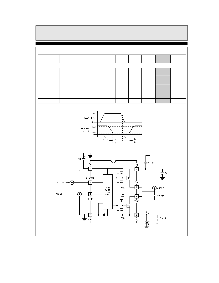
AC Electrical Characteristics
T
A
e
25 C unless otherwise specified
Parameter
Description
Test
Min
Typ
Max
Test
Units
Conditions
Level
Switching Characteristics (V
DD
e
V
H
e
12V V
L
e b
3V)
t
R
Rise Time
C
L
e
100 pF
4
25
IV
ns
C
L
e
2000 pF
20
t
F
Fall Time
C
L
e
100 pF
4
25
IV
ns
C
L
e
2000 pF
20
t
D-1
Turn-Off Delay Time
C
L
e
2000 pF
20
25
IV
ns
t
D-2
Turn-On Delay Time
C
L
e
2000 pF
10
25
IV
ns
t
D-1
3-State Delay
25
IV
ns
t
D-2
3-State Delay
25
IV
ns
Timing Table
7154 2
Standard Test Configuration
7154 3
3
TD
is
19in
EL7154C
High Speed Monolithic Pin Driver
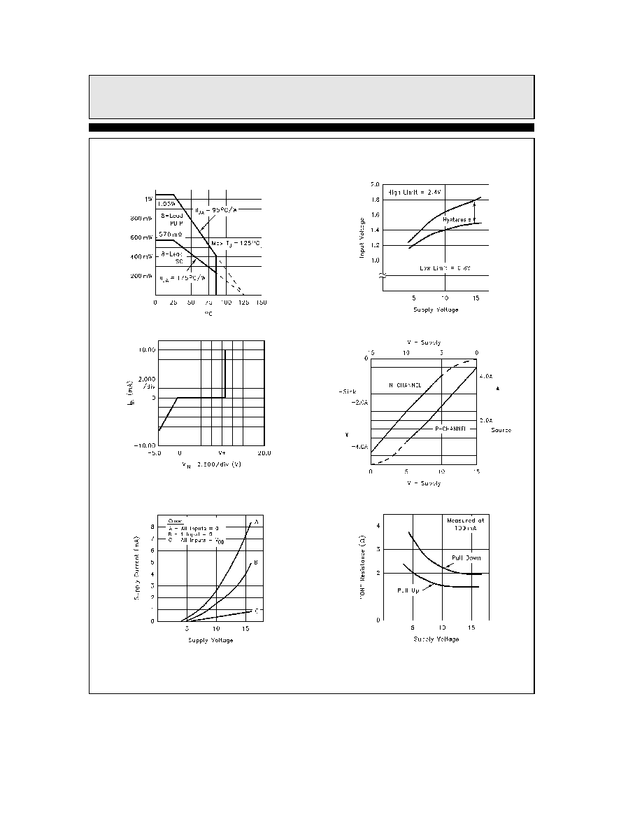
Typical Performance Curves
Max Power Derating Curves
7154 9
Supply Voltage
Switch Threshold vs
7154 10
Input Current vs Voltage
7154 11
Peak Drive vs Supply Voltage
7154 12
Quiescent Supply Current
7154 13
``ON'' Resistance vs Supply Voltage
7154 14
4
EL7154C
High Speed Monolithic Pin Driver
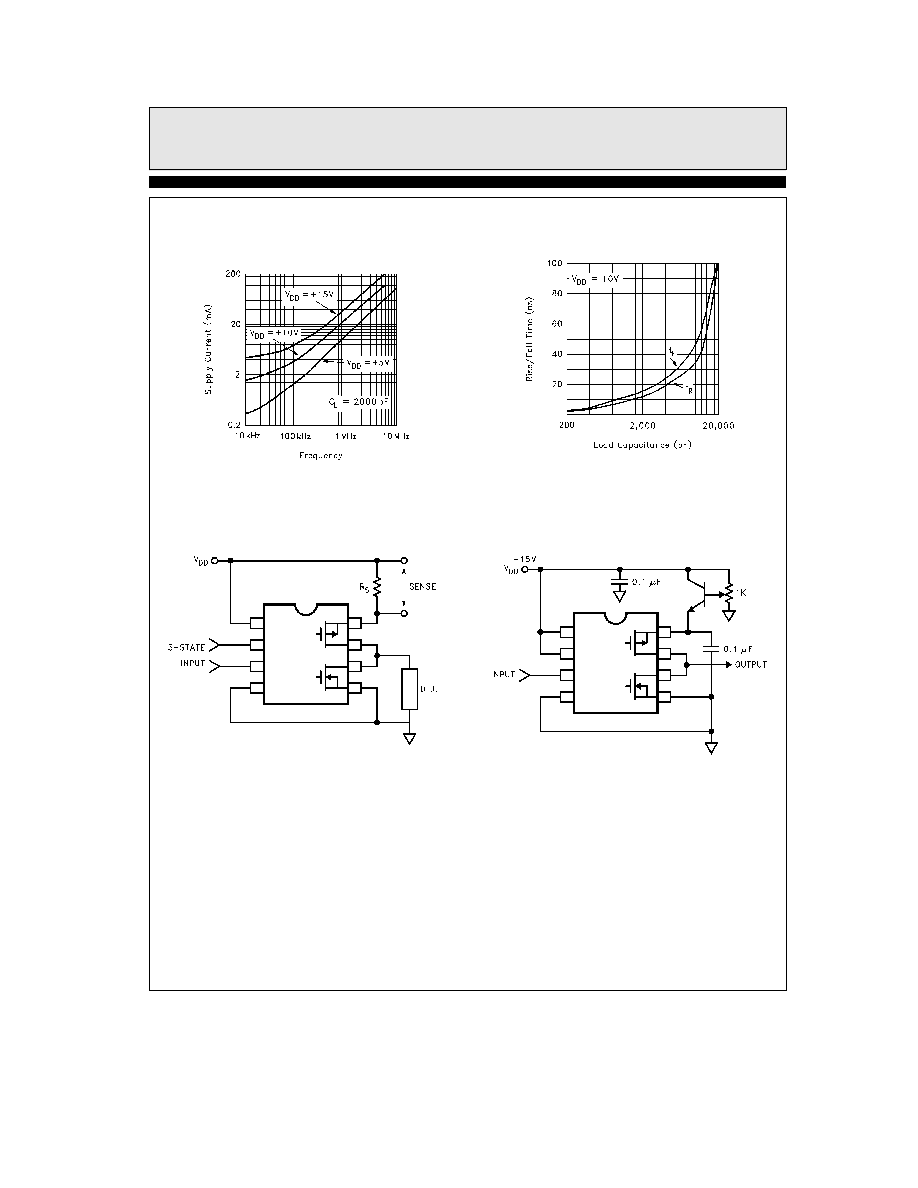
Typical Performance Curves
Contd
Average Supply Current vs
Voltage and Frequency
7154 15
Rise Fall Time vs Load
7154 16
Typical Applications
Pin Driver
7154 4
Adjustable Amplitude Pulse Generator
7154 5
5